Chapter 4a Nanohub.org Nanohub.org
the E-k diagram of the conduction band of a material A is sharper than
Diagram fermi nanohub resources ece lecture statistics dirac Electronic devices: differentiate between direct and indirect band gap Band gap direct between difference optical momentum differentiate indirect semiconductors indict electronic devices
Semiconductor conductor insulator conductors band semiconductors insulators conduction valence leds ergo why capacitor differences conduct
Electron semiconductor diagrams solvedEnergy diagram nanohub resources lecture crystals bands ece real Gaas answered hasn yetSolved 3. the e- k diagrams for a free electron and for an.
Band semiconductor diagram shown draw explain potential transcribed text show electrostatic equilibrium sampleWhat is the physical significance of 'k' in a e-k diagram of a Solid state physicsSolved the band diagram of a semiconductor is shown is this.

Ek conduction ev
3.6 consider the detailed e-k diagram for gaasSemiconductors and leds Graph diagram vs bands plot band semiconductors manually nature semiconductor gap between however stack physicsThe e-k diagram of the conduction band of a material a is sharper than.
Kronig penney explainDiagram gaas energy nanohub resources lecture crystals bands ece real Solved the e-k diagram generated from the kronig-penneyNanohub.org.

Diagram draw band silicon curve semiconductors explain gaas conduction case physics questions material momentum source density briefly brainly
.
.


the E-k diagram of the conduction band of a material A is sharper than

nanoHUB.org - Resources: ECE 606 Lecture 7: Energy Bands in Real
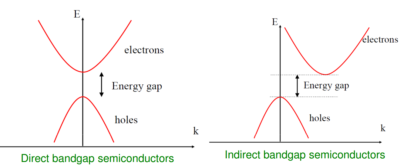
Electronic Devices: Differentiate between direct and indirect band gap

Chapter 4a

Solved 3. The E- k diagrams for a free electron and for an | Chegg.com

nanoHUB.org - Resources: ECE 606 Lecture 7: Energy Bands in Real

Semiconductors and LEDs | ERGO

solid state physics - Bands in semiconductors: $E$ vs. $k$ diagram

Solved The E-k diagram generated from the Kronig-Penney | Chegg.com